
As the semiconductor industry faces severe physical limits and diminishing economic returns from traditional silicon manufacturing, Huawei has proposed a radical shift in how future computer chips are designed and built.
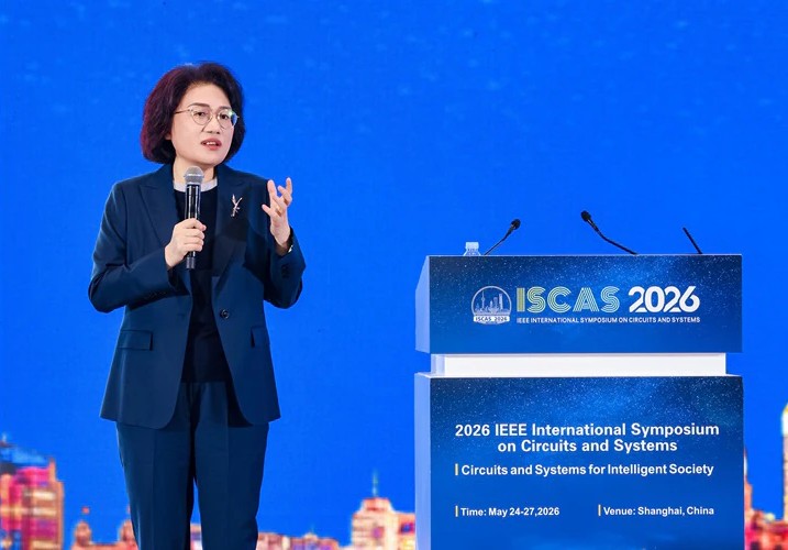
Speaking at the 2026 IEEE International Symposium on Circuits and Systems (ISCAS), He Tingbo, President of Huawei’s chip design unit, introduced the “Tau Scaling Law.” The new framework proposes replacing geometric scaling, the decades-long practice of physically shrinking transistors, with time Tau scaling as the core guiding principle for the next generation of semiconductors and electronic systems.
For more than fifty years, the global tech sector has relied on Moore’s Law to predictably double transistor density and performance. However, as physical constraints make shrinking transistors increasingly difficult and costly, the industry has experienced a severe slowdown in geometric progress. Huawei’s Tau Scaling Law addresses this bottleneck by focusing on the compression of signal propagation delays rather than physical size alone, aiming to steadily drive up performance, energy efficiency, and transistor density across multiple layers of technology.
To implement this principle, Huawei developed a multi-level co-optimization mechanism that spans devices, circuits, chips, and entire computing systems.
At the foundational physical layer, the approach optimizes the resistance and parasitic capacitance of transistors to minimize underlying delays. At the circuit level, Huawei introduced a novel architecture known as “LogicFolding.” This technology breaks the physical boundaries of traditional layouts to drastically shorten critical-path wiring, reducing the resistive and capacitive load of signal propagation while maximizing density.
On a broader scale, the methodology utilizes a full-stack coordinated design of software, architecture, and silicon to achieve precise, workload-driven control over instruction and data flows. At the system level, Huawei is redefining interconnect protocols with a technology called UnifiedBus, which aims to achieve unified memory addressing and native memory semantics for massive computing clusters (SuperPoDs), drastically slashing system communication latency.
While the framework represents a major conceptual shift, the company indicated that the underlying principles are already operational. Over the past six years, Huawei has designed and mass-produced 381 chips utilizing the Tau Scaling Law across various market sectors.
The strategy is poised for its first major consumer-facing test later this year. Huawei confirmed that its upcoming Kirin smartphone chips, scheduled to launch in Fall 2026, will be the first commercial hardware to officially feature the LogicFolding architecture to boost real-world performance.
Acknowledging the immense challenges of modern semiconductor evolution, He emphasized that the path forward cannot be traveled alone.
“We believe that openness and collaboration are key to driving ongoing progress in the semiconductor industry,” He said during her keynote address. “No single company can independently find all the answers along the path of semiconductor evolution. With the Tau Scaling Law, we look forward to working closely with scientists, engineers, and industry partners around the